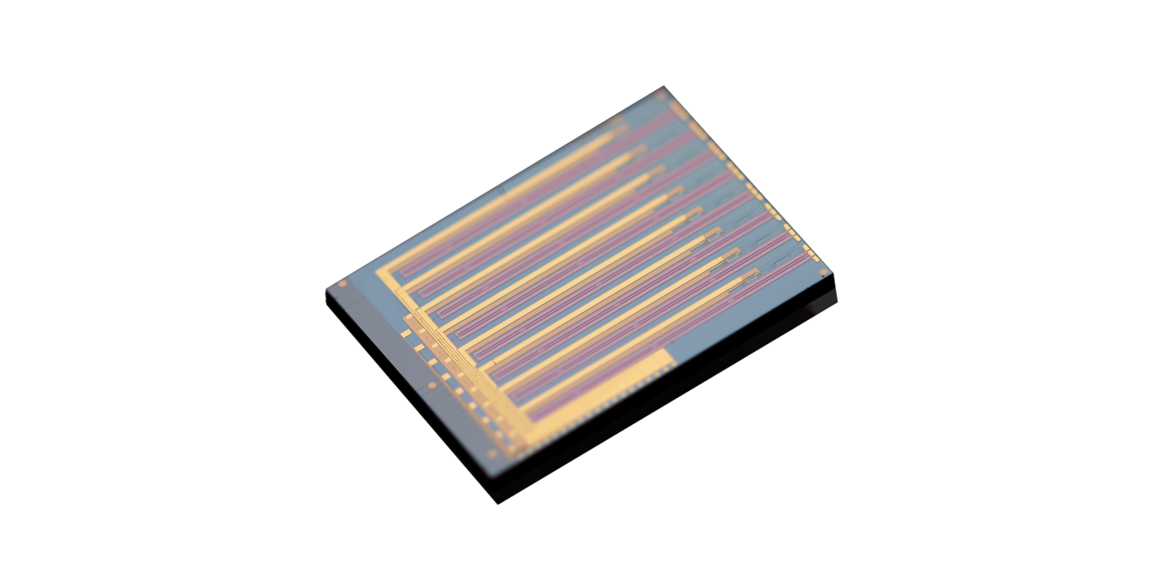
A high-speed optical engine brings electrical drive, optical modulation, laser power, coupling, thermal control, and fiber attachment into a compact assembly. The photonic chip is central, but it cannot be selected in isolation. They begin with lane rate, reach, modulation format, power envelope, and package boundary, then convert those needs into measurable device requirements.
Current roadmaps include 800G DR4, 1.6T DR8, 3.2T DR8, and coherent ZR modules. Each format distributes function differently across the driver, modulator, laser, receiver, and digital processor. Multi-channel circuits may reduce component count, while bare dies provide custom integration freedom.
The preferred route depends on capability, yield, and ownership of difficult interfaces. Electrical and optical simulation models are correlated to prototypes, allowing later engine revisions to reuse validated assumptions instead of restarting every interface study.
For engine development, available TFLN chips reach 70 to 110 GHz and include multi-lane direct-detection products, coherent IQ circuits, and a bare intensity die. From an engine perspective, these examples show where thin-film lithium niobate can strengthen an optical engine, while requiring packaged performance, process distributions, reliability evidence, and a credible scale-up plan.
Optical Engine Architecture Determines the Required Chip Format
In a direct-detection design, a TFLN photonic chip converts several high-speed electrical lanes into intensity-modulated optical outputs. They define the lane count, electrical drive mode, laser distribution, coupling arrangement, and required extinction.
Multi-lane integration can reduce alignments, but channel imbalance, skew, crosstalk, or one weak lane may affect the entire engine yield. Within coherent engines, TFLN chips perform more complex amplitude and phase operations. A PDMIQ circuit can support ZR-class formats, but it adds path balance and bias requirements.
They coordinate driver swing, DSP assumptions, polarization handling, and control loops before fixing the die, because the chip and electronics together determine waveform quality and transmitter power. A bare intensity-modulator die creates another partition.
It lets them design custom RF launches, optical coupling, and mechanical integration around the engine, potentially improving density. In exchange, their team or package partner assumes responsibility for alignment, stress, thermal behavior, reliability, and final test. This trade should be decided with capability and cost data, not footprint alone.
Bandwidth and Voltage Must Be Balanced with Loss and Coupling
The listed 3.2T DR8 TFLN photonic chip offers 110 GHz bandwidth, insertion loss below 14 dB including coupling, differential half-wave voltage below 1.5 V, and extinction above 25 dB. They translate these values into driver energy, laser power, receiver margin, and expected channel distribution before assessing whether the engine meets its total budget.
Other TFLN chips address 1.6T DR8 or 800G DR4 at 70 GHz, with coupling-inclusive loss below 14 dB and differential voltage below 2 V. The lower nominal bandwidth may still be appropriate for the waveform and package.
They compare measured large-signal performance rather than assuming that the upper frequency option provides the selected efficiency or yield. The coherent PDMIQ device is listed at 70 GHz, below 7 dB insertion loss, below 4.5 V differential half-wave voltage, and above 25 dB extinction. A bare intensity die reaches 110 GHz below 5 dB loss and 3 V.
These devices integrate different functions, so their cost and performance comparison normalizes package responsibility and external optical components. They track assembly learning curves and capital utilization, since a package that performs well may remain uneconomic until alignment time and rework rates improve.
Packaging, Test, and Supply Controls Enable Volume Deployment
Volume adoption of a TFLN photonic chip requires a defined package and assembly flow. They review fiber-array tolerances, coupling method, RF interconnect, die attach, thermal interface, contamination control, and rework policy.
Pilot builds measure yield at each stage, identifying whether the economic bottleneck lies in the wafer, alignment, high-frequency connection, or final calibration. TFLN chips should also be designed into a layered test strategy. Wafer screening removes obvious defects, package testing verifies coupling and electro-optic response, and module testing confirms link behavior.
Correlation among these stages allows earlier fault isolation. They require serial traceability and continuous data so that a later module failure can be connected to its manufacturing history. Supply readiness includes wafer capacity, package-partner capacity, equipment lead time, quality systems, and process-change notification.
They assess how rapidly the chain can ramp and how variation will be communicated. High-speed engines often share specialized materials and tools, so one constrained step can govern delivery even when the chip fabrication itself appears scalable.
Customer samples are built with production-intent materials and tooling, reducing the risk that qualification approves a configuration that cannot be sustained during ramp. At engine level, thin-film lithium niobate chips can support high-speed optical engines through wide bandwidth, manageable drive voltage, and multi-channel or coherent circuit options.
Their actual contribution is determined after optical loss, package transitions, thermal behavior, controls, and manufacturing variation are included. Engine-level evidence remains the basis for a credible selection.
Their development path uses common reference boards, packaged prototypes, multi-lot characterization, reliability tests, and pilot assembly. They connect every device metric to a module margin or production control. This approach identifies where integration creates real power or density benefits and where it merely transfers difficult work to another organization or manufacturing stage.
An optical engine succeeds through coordination among the chip, driver, laser, coupling, thermal controls, and test process. A complete assembly using a Liobate TFLN chip can expose operating margin, yield behavior, and supply constraints before volume planning.
